Arc Plasma Source
APS-1
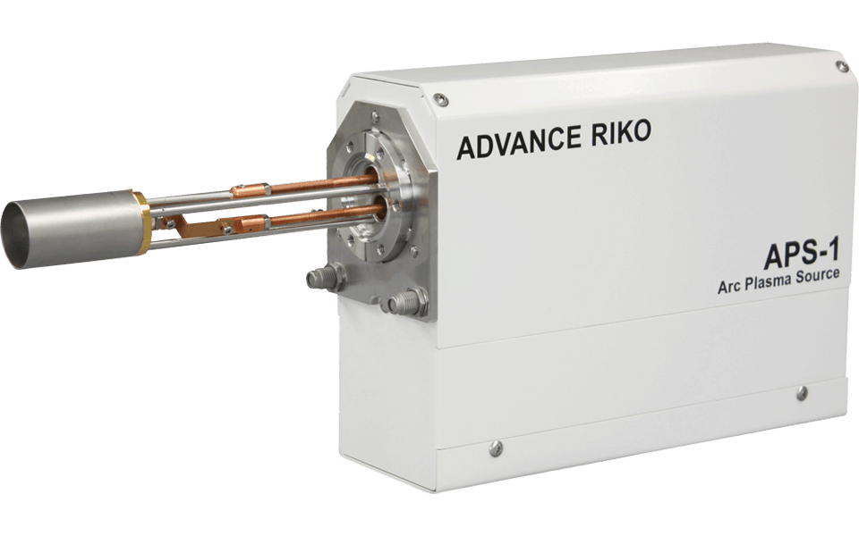
Simultaneous deposition of different “targets”
By adding this source to APD series or your vacuum chamber, different “targets” can be deposited simultaneously and materials with new characters can be produced.
Applications
- Produce chemical compounds from multiple depositions
- Add to your vacuum chamber
Features
- Due to size uniformity of nanoparticles compared with ones produced through previous wet process, highly active catalysts can be produced.
- Capable of selecting nanoparticle diameter from approx.1.5nm to 6nm
- Capable of generating easily oxide and nitride by changing atmosphere
- Attachable to a vacuum flange of ICF070 (VG50) or equivalent without any consideration of which direction
- Easy maintenance because no water cooling facilities are needed
Specifications
| Target size | φ 10 × L 17 (mm) |
|---|---|
| Substrate size | φ 2 inch (φ 50 mm) |
| Deposition rate | 0.01 ~ 0.3 nm/s *1 |
| Film thickness uniformity | Fe: < ± 10 % (φ 20mm area) *1 |
| Materials Available for deposition | Conductive materials *2 |
*1 Distance from a target to a substrate: 80mm
*2 Specific resistance of a target: 0.01Ωcm or less
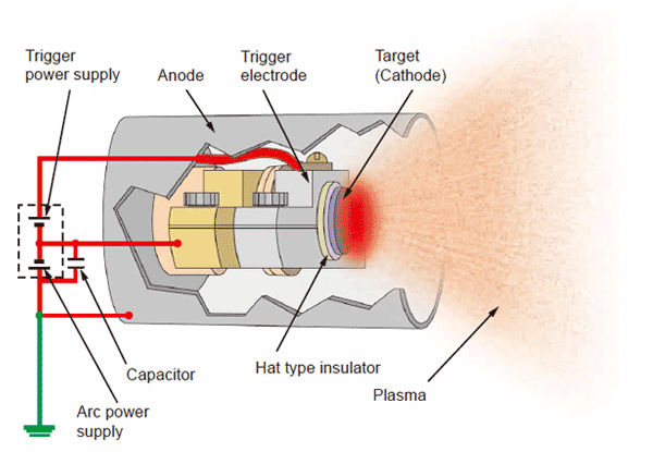
Schematic of the Arc Plasma Source(APS)
Utility
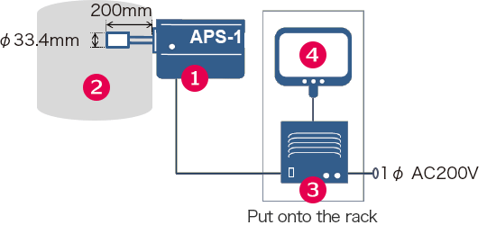
- Power requirement:AC200V Single phase ±10% 2kVA
- Dimension
- ❶ Condenser box:W110 x D320 x H200 (mm)
- ❷ Body of APS within vacuum chamber:φ34 x L200 (mm)
- ❸ Power supply unit:W200 x D360 x H200 (mm)
- ❹ Controller:W240 x D400 x H200 (mm)
*Put power supply unit & controller onto the rack.
TEM Images for Nano-Particles prepared by APS

TEM image of Pt nano-particles supported on
Well-dispersed Pt nano-particles on the carbon powder are deposited.
TEM image of Pt nono-particles on a substrate
The size of nano-particle becomes larger as the pulse number of arc plasma shots is increased.
TEM image of Pt thin film
Extremely thin Pt film is formed by a stacking of nano-particles.
Photos of Deposition System installing APS
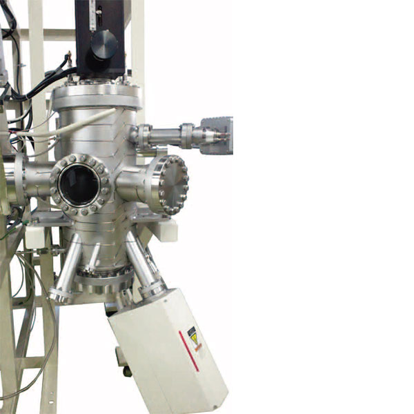

Table 1 Elements checked for deposition
| 1A | 2A | 3A | 4A | 5A | 6A | 7A | 8 | 1B | 2B | 3B | 4B | 5B | 6B | 7B | 0 | |||
| 1 | H | He | ||||||||||||||||
| 2 | Li | Be | B | C | N | O | F | Ne | ||||||||||
| 3 | Na | Mg | Al | Si | P | S | Cl | Ar | ||||||||||
| 4 | K | Ca | Sc | Ti | V | Cr | Mn | Fe | Co | Ni | Cu | Zn | Ga | Ge | As | Se | Br | Kr |
| 5 | Rb | Sr | Y | Zr | Nb | Mo | Tc | Ru | Rh | Pd | Ag | Cd | In | Sn | Sb | Te | I | Xe |
| 6 | Cs | Ba | Lanthanoid | Hf | Ta | W | Re | Os | Ir | Pt | Au | Hg | TI | Pb | Bi | Po | At | Rn |
| 7 | Fr | Ra | Actinoid | |||||||||||||||
Checked Limited in use
Analysis service by using this product
Related product
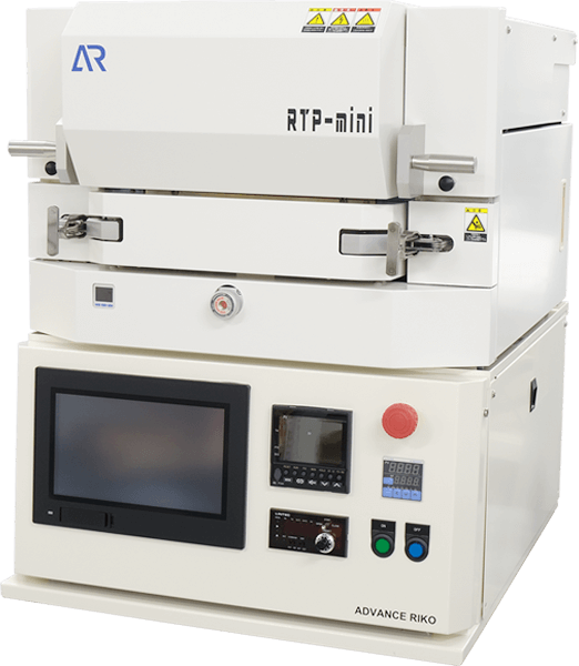
Infrared lamp heating system RTP-mini
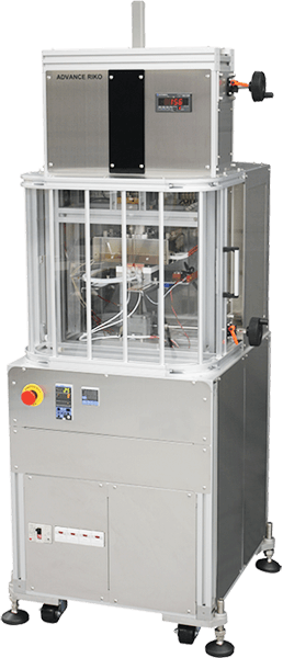
Thermal Flow Rate Evaluation System for Low Thermal Resistance Multilayer Substrates F-CAL
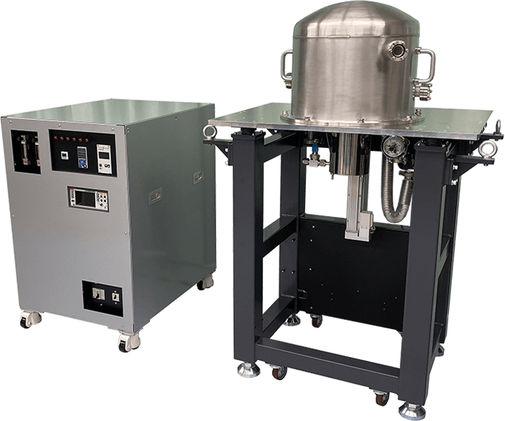
Ultra High Precision Thermal Expansion Measurement System by Laser Interferometer SuperLIX
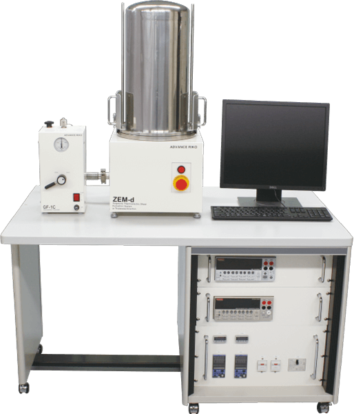
Polymeric Thermoelectric Sheet Evaluation System ZEM-d
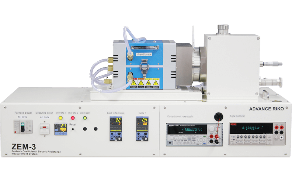
Seebeck Coefficient / Electric Resistance Measurement System ZEM-3 series
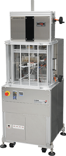
Atmospheric Thermoelectric Module Evaluation System F-PEM
Arc Plasma Source APS-1 Contact form
The information that you enter will only be used to provide you with a response. However, when you request that we mail you a catalog or other materials, please understand that the shipper specified by ADVANCE RIKO may use only the information necessary to send those materials, such as your name and address.
Please check our privacy policy for more details.